| dc.contributor.author | Сычик, В. А. | ru |
| dc.contributor.author | Уласюк, Н. Н. | ru |
| dc.coverage.spatial | Минск | ru |
| dc.date.accessioned | 2023-12-21T07:32:30Z | |
| dc.date.available | 2023-12-21T07:32:30Z | |
| dc.date.issued | 2023 | |
| dc.identifier.citation | Сычик, В. А. Полупроводниковый светодиодный элемент = Semiconductor led element / В. А. Сычик, Н. Н. Уласюк // Приборостроение-2023 : материалы 16-й Международной научно-технической конференции, 15-17 ноября 2023 года, Минск, Республика Беларусь / редкол.: О. К. Гусев (пред.) [и др.]. – Минск : БНТУ, 2023. – С. 89-90. | ru |
| dc.identifier.uri | https://rep.bntu.by/handle/data/138644 | |
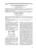
| dc.description.abstract | Полупроводниковый светодиодный элемент, содержащий p- и n-слой, омические контакты к ним, выполнен p-i-n структурой из широкозонного полупроводника с сильнорегированными p+- и n+- слоями толщиной (0,7–0,9)Ld, а толщина i-слоя собственной проводимости равна (1,1–1,6)Ld, где Ld – диффузионная длина носителей заряда. | ru |
| dc.language.iso | ru | ru |
| dc.publisher | БНТУ | ru |
| dc.title | Полупроводниковый светодиодный элемент | ru |
| dc.title.alternative | Semiconductor led element | ru |
| dc.type | Working Paper | ru |
| local.description.annotation | A semiconductor LED element containing a p- and n-layer, ohmic contacts to them, is made of a p-i-n structure from a wide-gap semiconductor with highly regulated p+- and n+- layers with a thickness of (0.7–0.9)Ld, and the thickness of the i-layer intrinsic conductivity is equal to (1.1–1.6)Ld, where Ld is the diffusion length of charge carriers. | ru |